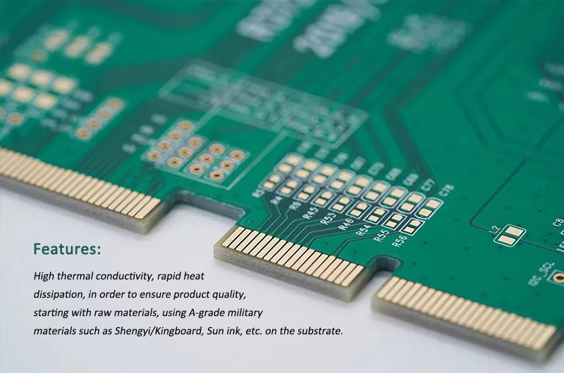
At present, there are many gold fingers on many pcb circuit boards, which are used to insert into the card slot and contact with the metal spring sheets in the card slot. The pads arranged in a similar arrangement of fingers, because this type of design has a great effect on the wear resistance and conductivity of the pad surface. Higher requirements, so a layer of nickel and a layer of gold will be plated on the surface of the pad, so it is commonly called gold finger.
Through the contact between the gold finger and the spring sheet in the card slot, the interconnection between the external PCB and the main board is realized, and at the same time, it is easy to disassemble and replace due to the difference in performance requirements of users. The most common gold finger design appears on the graphics card and memory stick in the computer.
Gold-plated gold-finger circuit boards actually refers to thick gold, hard gold, also known as plug gold-plated, not gold-plated or flexible boards. The characteristics of this kind of gold are that it is relatively hard, can be plated very thickly, and is resistant to plugging and unplugging. Many times the gold finger card board we hear refers to this type of board.
Hard gold has better wear resistance, and can ensure that 20,000 times of insertion and removal will not affect the quality, and the gold thickness must be more than 5U”. However, the hard gold processing technology is relatively complex, and the gold thickness requires high consumption of more gold salt, which directly causes the cost to be too high.

Specification of 12 layer gold finger graphics card pcb circuit board
Material: TU872
Layers: 12 layers
Copper Thickness: 1oz
Plate thickness: 1.6mm
Minimum drilling: 0.1mm
Minimum line width: 0.065mm
Minimum line spacing: 0.065mm
Surface Treatment: Immersion Gold and Gold Finger
Features: High thermal conductivity, rapid heat dissipation, in order to ensure product quality, starting with raw materials, using A-grade military materials such as Shengyi/Kingboard, Sun ink, etc. on the substrate.
Application of 12 layer gold finger graphics card pcb circuit board
12-layer gold finger graphics card pcb circuit board is often used in communication equipment, electronic equipment, smart home, manufacturing and other fields.

